(Hong Kong)

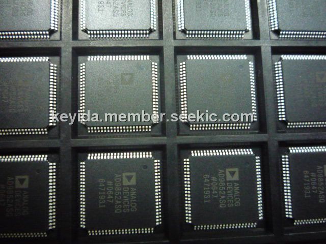

Product Summary
The AD9852ASQ digital synthesizer is a highly integrated device that uses advanced DDS technology, coupled with an internal high-speed, high-performance D/A converters and a comparator to form a digitally-programmable agile synthesizer function. When referenced to an accurate clock source, the AD9852ASQ generates a highly stable, frequency-phase amplitude-programmable sine wave output that can be used as an agile L.O. in communications, radar, and many other applications. The AD9852ASQ’s innovative high-speed DDS core provides 48-bit frequency resolution (1 micro Hertz tuning steps). Phase truncation to 17 bits assures excellent SFDR. The applications of the device include Agile, L.O. Frequency Synthesis, Programmable Clock Generator, FM Chirp Source for Radar and Scanning Systems, Test and Measurement Equipment and Commercial and Amateur RF Exciter.
Parametrics
AD9852ASQ absolute maximum ratings: (1)Compliance Range (V): 1V; (2)FS Iout (mA nom): 20mA; (3)I Supply total (max): 922mA; (4)Maximum Junction Temperature:150℃; (5)VS: 4V; (6)Digital Inputs: –0.7V to +VS; (7)Digital Output Current: 5mA; (8)Storage Temperature: –65℃ to +150℃; (9)Operating Temperature: –40℃ to +85℃; (10)Lead Temperature (Soldering 10 sec): 300℃; (11)Maximum Clock Frequency: 300 MHz.
Features
AD9852ASQ features: (1)300 MHz Internal Clock Rate ; (2)Integrated 12-Bit Output DACs; (3)Ultrahigh-Speed, 3 ps RMS Jitter Comparator; (4)Excellent Dynamic Performance: 80 dB SFDR @ 100 MHz (61 MHz) AOUT; (5)43 to 203 Programmable Reference Clock Multiplier; (6)Dual 48-Bit Programmable Frequency Registers; (7)Dual 14-Bit Programmable Phase Offset Registers; (8)12-Bit Amplitude Modulation and Programmable; (9)Shaped On/Off Keying Function; (10)Single Pin FSK and PSK Data Interface; (11)Linear or Nonlinear FM Chirp Functions with Single Pin Frequency “Hold” Function; (12)Frequency-Ramped FSK<25 ps RMS Total Jitter in Clock Generator Mode; (13)Automatic Bidirectional Frequency Sweeping SIN(x)/x Correction; (14)Simplified Control Interface; (15)10 MHz Serial, 2-Wire or 3-Wire SPI-Compatible; (16)100 MHz Parallel 8-Bit Programming; (17)3.3 V Single Supply; (18)Multiple Power-Down Functions; (19)Single-Ended or Differential Input Reference Clock; (20)Small 80-Lead LQFP Packaging.
Diagrams

| Image | Part No | Mfg | Description |  |
Pricing (USD) |
Quantity | ||||
|---|---|---|---|---|---|---|---|---|---|---|
 |
 AD9852ASQ |
Analog Devices Inc |
IC DDS DUAL DAC W/COMP 80-LQFP |
Data Sheet |
Negotiable |
|
||||
|
AD9852ASQZ |
Analog Devices Inc |
IC DDS DUAL DAC W/COMP 80-LQFP |
Data Sheet |
Negotiable |
|
||||